


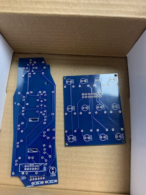
Printed Circuit Boards (PCBs) or Printed Wiring Boards (PWB) are board structures that must provide electrical conductor paths that interconnect the components placed/ mounted on them.
Getting a fast PCB prototype is crucial in the product development process. APOLLOPCB is a recommended professional and trustworthy PCB prototype manufacturer that delivers PCBs in just 3-5 days.
Classes of PCB Designs
Generally, PCBs divided into two classes, depending on the material, design requirements, and functions. The first class is RF, Microwave, Analog PCBs while the second class is digital-based PCBs,.
RF, Microwave, Analog PCB vs. Digital-based PCBs
Parameter | RF, Microwave, Analog PCBs | Digital-based PCBs |
Circuit Complexity | Has low circuit complexity
| Has high circuit complexity |
No of Components | Has less number of components | Has a higher number of components |
No of Leads | It has less number of leads, because it uses components like resistor, capacitor, transformer and etc. , which have 2 or 3 leads. | Digital components have a large number of leads, and this leads to the circuit having complex interconnections |
Number of layers | Only one/two layers | Requires multiple layers because of the many components it uses |
Signal losses | Minimizing signal losses is essential | Digital PCBs have a high tolerance for losses and more noise immunity. |
Dielectric constants of components on PCB | Low/uniform dielectric constants are needed. Components with non-uniform dielectric constants when used on RF PCBs, cause phase distortion | Compared to RF PCBs, losses in the dielectric are not much of a concern. |
PCB design | Physical tools that provide high accuracy and convenient graphical manipulation of PCB shapes are needed. | PCB design must be optimized to ensure accuracy in making a large number of connections. |
Coupling | Two traces running side by side can be used as directional couplers and transfer a signal from one circuit to the neighboring circuit. | Coupling between parallel traces in digital PCBs can cause a malfunction. |
The PCB Assembly Design Process
It is a flowchart of steps taken to produce a PCB that matches the desired end product and functions properly over all the normal variations in component values, tolerance, speeds, temperature tolerance, and more.

1. The System Specification:
This is the initial step carried out by the designer. The designer lists out the function(s) of the desired end product, the conditions which it will operate under, development costs and schedule, size, weight, repair protocols and more.
2. Create a system block diagram:
Here, the designer breaks the overall function(s) of the system into parts and depicts them in a block diagram to illustrate how the system’s processes link with each other.
3. Partition the system into PCBs:
The different circuits carrying out the system’s functions are divided into PCB assemblies, and circuits that must work together to carry out a function grouped together onto a single PCB.
4. Creating a schematic:
At this stage, the designer chooses the components to be used and then creates a schematic. A schematic is created using CAE (Computer Aided Engineering) systems, it shows a detailed connection between components.
5. Simulating the design:
After the desired schematic is created, component libraries are made for the components used in the schematic. Component libraries contain information, such as the size of the component, packaging, the lead spacing size, function of each pin and etc. This information is required by PCB design tools. The design is then simulated and debugged and until the required logical and gross timing specifications are met.
6. Virtual Assembly:
After the defects found by the simulator are corrected, the actual physical layout of the design is initiated. Components are mounted either manually by the designer using graphic-based tools or automatically by tools like the PCB CAD system.

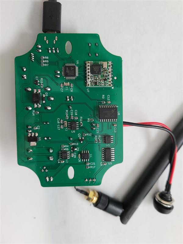
APOLLOPCB virtual assembly process
The placement operation is done in a pattern where components that work together to carry out a logical function are grouped together, and groups of components used in functions that interact are placed adjacent to each other.
After the placement operation, we sequence/ schedule. Scheduling/ Sequencing is the necessary arrangement of connections between components to avoid problems like coupling and reflections. The connections are called nets.
Lastly, we simulate the physical layout design. The placement operation gives us the x-y location of the nets. This information is used to estimate the high-speed characteristics of the nets and therefore predict the reflection and coupling associated with each net. If the simulation process reveals excessive noise or reflection, then we have to go back to the placement step and reposition some of the components.
The simulation of the physical layout is very important because it enables the designer to see and correct any malfunctions before routing is done.
1. Routing the PCB:
First of all, the Routability Analysers in the CAD systems are used to check if the design will fit in the proposed signal layers. Depending on the cost goal mentioned in step one, system specification, the designer can have a limited number of signal layers to work with.After getting successful routability results, we route the PCB. Routing the PCB means fitting all the connections into the signal layers in the form of the copper traces, carefully following the spacing and length rules.
8. Inspection and Soldering:
The physical data of the routed PCD is checked one last time to verify that the design meets the system requirements mentioned in step one. Soldering is a joining process where the component leads are joined to the board. Prior to Soldering, the leads of the components must be cropped to an appropriate length depending on the soldering technique used.
Do you need a Fast, Reliable, and Affordable PCB Prototype & Assembly Service?
") We recommend using APOLLOPCB.
We recommend using APOLLOPCB.
APOLLOPCBis one of the most experienced PCB-Prototype and PCB-Assembly manufacturers in China. It has more than 10 years in the PCB-Prototype and PCB-Assembly manufacturing industry. They offer high-quality PCB material, on-time shipping at reasonable prices. They also custom design boards according to one’s needs.
Why should you choose APOLLOPCB?
")
→Delivers using DHL in just 3-5 days.
→99% on-time shipping by DHL.
→ 24 hour online customer service.
→Guaranteed quality from PCB quote to delivery.
→Minimum orders starts from 1pcs for PCBA.
Summary
In this section, we learned about the definition of PCB, the characteristic of the Analog-based PCBs and Digital-base PCBs. The two differ based on circuit complexity, components used, PCB design requirements, and applications.
Lastly, we covered the PCD design process, which is basically a flowchart of 10 steps that describe how a PCB is engineered. Do you remember the 8 steps?
This article is originally published on electronicslovers.com and authorized to reprint on APOLLOPCB.
-
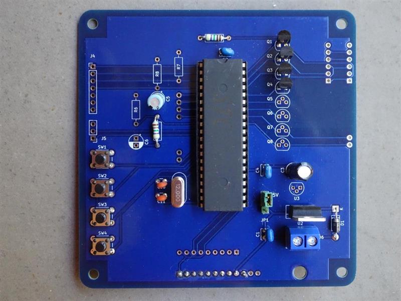 89C52 clock boardVery well manufactured. HASL was easy to solder to and the soldermask was smooth and properly cured. I liked that APOLLOPCB c270 0 Mar 24. 2021, 11:10:56
 -
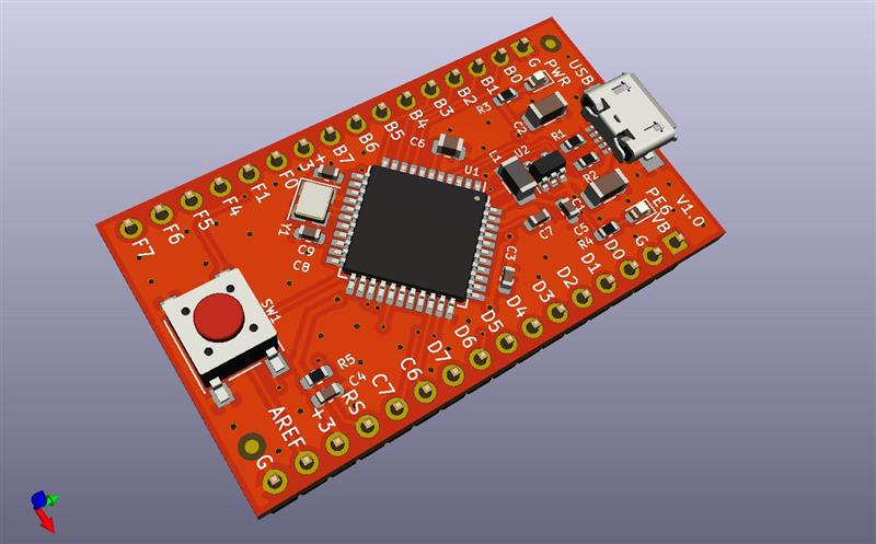 ATmega32U4 breakout board - assembledEven though this board has much less components than my previous designs I decided to test APOLLOPCB's assembly service.299 0 Mar 24. 2021, 11:10:56
 -
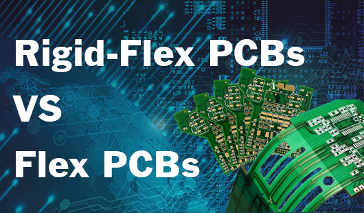 Flex and Rigid-Flex PCBs – APOLLOPCB’s PCB Manufacturing CapabilitiesIntroduction: Printed circuit boards come in many forms, shapes and sizes. PCBs can be distinguished on the basis of fre174 0 Mar 24. 2021, 11:10:56
 -
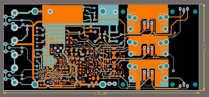 HV Amplifier's PCBI was astonished of the professional service received so far, moreover for my last order when I was asking to do as fast as p155 0 Mar 24. 2021, 11:10:56
 -
 newvisionvery good quality very fast !!263 0 Mar 24. 2021, 11:10:56
 -
 APOLLOPCB will hold most of the service prices stableThe prices of PCB raw materials and electronic components for PCB assembly have been rising significantly worldwide recently,132 0 Mar 24. 2021, 11:10:56
 -
 PCBA (SMT)Betty worked with me refining the BOM and component availability, suggesting alternative. Great support!185 0 Mar 24. 2021, 11:10:56
 -
 Weather sensor shieldPCB arrived promptly. All boards were perfect, finished to a very high standard, look great and they even sent me an extra bo171 0 Mar 24. 2021, 11:10:56
 -
 Nice to meet you in L&B Frankfurt 2024The modern building is intelligent, connected and as a result saves energy. In combination with alternative energy sources and efficient lighting solutions, emissions in the building sector can be drastically reduced. This makes a significant contribution to achieving climate targets. 2,169 exhibitors presented the latest developments in building technology and trends in innovative lighting design at Light + Building in Frankfurt am Main from 3 to 8 March 2024. Over 151,000 visitors travelled to the world's leading trade fair for lighting and building-services technology.1 0 Mar 24. 2021, 11:10:56
 -
 Where to get a fastest PCB Assembly prototype?Printed Circuit Boards (PCBs) or Printed Wiring Boards (PWB) are board structures that must provide electrical conductor path111 0 Mar 24. 2021, 11:10:56


 Whatsapp 0086 755 29438407
 Mail info@apollopcb.com
  Tel 0086 755 29438407


