-
- PCB TYPE
- PRINTED CIRCUIT BOARD PROTOTYPE ALUMINUM PRINTED CIRCUIT BOARD R&F PCB FPC HIGH FREQUENCY PCB HIGH-TG PCB HEAVY COPPER PCB HDI PCB PCB FOR LIGHTING METAL CORE PCB
time:Jul 07. 2021, 09:00:59 Views:158
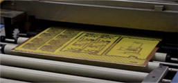
Manufacturing PCB circuit boards involves several complicated processes.
1: Film exposure: In this process, the mask or photomask is combined with chemical etching to subtract the copper area from the PCB circuit board substrate. Use the CAD PCB software program to create the photomask using the photo plotter design. The photomask was also created using a laser printer.
2: Laminating: Multi-layer PCB circuit boards are composed of multiple thin layers of etched boards or trace layers, which are bonded together through a lamination process.
3: Drilling: Each layer of the PCB circuit board needs the ability to connect one layer to another; this is achieved by drilling a small hole called "VIAS". Drilling is mainly done by using an automatic computer-driven drilling machine.

4: Solder pad spray tin: spray tin or chemical immersion gold on the solder joints of the electronic components on the solder pads on the PCB circuit board to solder the electronic components. Bare copper is not easy to solder. It requires the surface to be plated with materials that are convenient for welding. Earlier lead-based tin was used to plate the surface, but with R oHS (Restriction of Hazardous Substances) compliance, newer lead-free materials such as nickel and gold are now used for electroplating.
5: Test the PCB circuit board: Before soldering the electronic components to the PCB circuit board, it needs to be tested. The test can use a test rack tester or a pin test, which is a circuit board test device operated by other computers.
Whether it is PCB circuit board proofing or mass manufacturing, the manufacturing process and process procedures are similar, but the cost of manufacturing PCB circuit board samples is different from the pre-tool cost shared during mass manufacturing.

Got project ready to assembly? Contact us: info@apollopcb.com


We're not around but we still want to hear from you! Leave us a note:

Leave Message to APOLLOPCB
