-
- PCB TYPE
- PRINTED CIRCUIT BOARD PROTOTYPE ALUMINUM PRINTED CIRCUIT BOARD R&F PCB FPC HIGH FREQUENCY PCB HIGH-TG PCB HEAVY COPPER PCB HDI PCB PCB FOR LIGHTING METAL CORE PCB
time:Jan 10. 2022, 15:44:18 Views:167
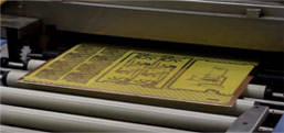
High frequency microwave PCB circuit board exposure has two types: line exposure and solder mask exposure. The function is to cure the irradiated local area through ultraviolet light irradiation, and then develop it to form a circuit pattern or a solder resist pattern.
The process of circuit exposure is to put a photosensitive film on the copper clad board, and then put it together with the circuit pattern negative and expose it with ultraviolet rays. The photosensitive film irradiated by ultraviolet rays will undergo polymerization reaction. The photosensitive film here can resist Na2CO3 weak alkali during development. The solution is washed away, and the non-sensitized part will be washed away during development. In this way, the circuit pattern on the negative film is successfully transferred to the copper clad board;

The process of solder mask exposure is the same: apply photosensitive paint on the circuit board, and then cover the area that needs to be soldered during exposure, so that the pads are exposed after development.

Got project ready to assembly? Contact us: info@apollopcb.com


We're not around but we still want to hear from you! Leave us a note:

Leave Message to APOLLOPCB
