-
- PCB TYPE
- PRINTED CIRCUIT BOARD PROTOTYPE ALUMINUM PRINTED CIRCUIT BOARD R&F PCB FPC HIGH FREQUENCY PCB HIGH-TG PCB HEAVY COPPER PCB HDI PCB PCB FOR LIGHTING METAL CORE PCB
time:Aug 20. 2021, 16:07:46 Views:193
Common FR-4 material PCBs are generally divided into three types: single-sided, double-sided and multi-layer boards. The names of factories with different production processes are different, but the principle of the process is the same, but they are called Hong Kong-funded enterprises, Taiwan-funded enterprises and foreign-funded enterprises.
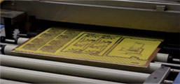
The single-panel process is simpler than the double-panel process. It is basically cutting---drilling---graphic transfer---etching---soldering and printing---metal surface treatment-- Finished product molding---test and inspection---packaged and shipped.

The general process of the panel: cutting ----- drilling-electroless copper (PTH) and electroplating a copper-pattern transfer (line)-pattern plating (two copper) and Protective tin plating-etching (SES)-intermediate inspection-solder mask (Solder Mask)-printed characters-metal surface treatment-finished product Forming-----Electrical test----Appearance inspection (FQC/OQA)----Packing and shipping.
The multi-layer board process is to add the inner layer process in front of the double-sided board process. The basic process: cutting material-----inner layer pattern transfer-----inner layer etching (DES)-----inner layer etching Inspection/AOI-----Cu surface oxidation treatment (blackening or browning)-layout and stacking-pressing (pressing board)-cutting board forming-- ---Following the double-sided board process

Got project ready to assembly? Contact us: info@apollopcb.com


We're not around but we still want to hear from you! Leave us a note:

Leave Message to APOLLOPCB
