-
- PCB TYPE
- PRINTED CIRCUIT BOARD PROTOTYPE ALUMINUM PRINTED CIRCUIT BOARD R&F PCB FPC HIGH FREQUENCY PCB HIGH-TG PCB HEAVY COPPER PCB HDI PCB PCB FOR LIGHTING METAL CORE PCB
Real PCB &PCB Assembly Manufacturer
IS09001:2015 Standard
UL.RoHS. REACH Certified
3000+ Orders/Day
99% on-time Shipping
100,000+ Customers
PCB panel refers to put several small PCBs into a large board for production. It is easy to separate the multiple PCBs and avoid damaging the boards in the process of the panel assembly. And the panel types are determined according to the shape of the single board.

Why need panel design when manufacturing PCBs?
· Improving fabrication efficiency
Some PCBs are too small to meet the requirements of SMT fixtures, put them into a large board is more convenient for manufacturing. And the SMT process of multiple PCBs can be run at the same time in automatic machines, then increase the utilization rate of machines.
· Good quality control
Automated production is conducive to quality control and improves the yield of fabrication.
· Reducing PCB assembly cost
Panel design is more suitable for automatic production line, which can save labor costs. And it helps to use the PCB area effectively and reduce materials waste by panel design for some different shaped PCBs.
undefined
Panel types of PCB assembly
· V-Scoring
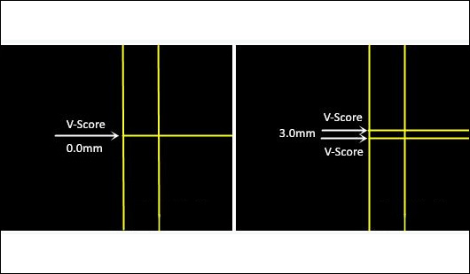
V-scoring also called as V-cut or V-groove, it is the most popular panel type nowadays. The V-shape line between each board is a connection of each board in the panel and easy to break. The space between each PCB usually can be 0.0mm or 0.3mm with V-Scoring techniques, and the recommended V-cut angle is 30°.
V-cut is suitable for the regular panel design, and the cut line should be horizontal and vertical lines. For this panel type, the minimum size of the boards should be 75mm*75mm.
· Routing slot/milling slot +Tab (Tab-routing)
Routing slot includes two types:
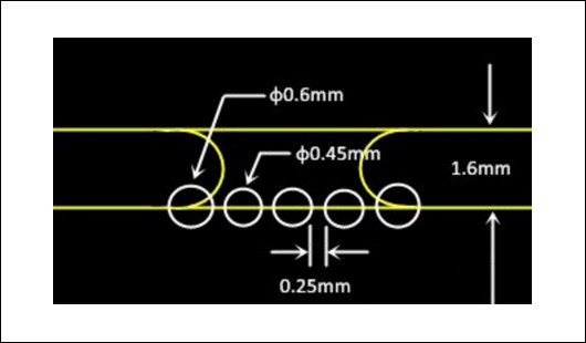
--Tab-routing with breaking holes (stamp holes)
This panel type also named as stamp holes and is usually used in the special-shaped PCBs, like round-shaped boards.
The space between each PCB for this panel type should be 1.6mm; the hole spacing is generally greater than 0.25mm, and the hole diameter should be greater than 0.45mm.
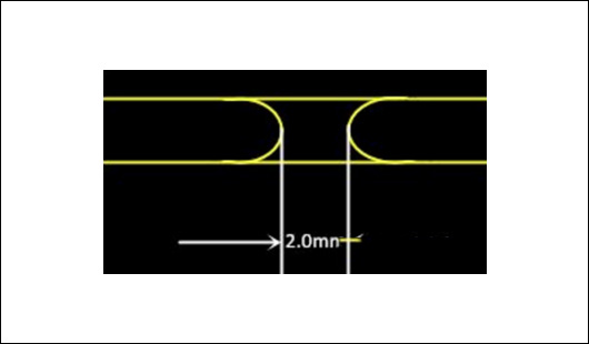
--Tab-routing without holes
The width of the tab should at least be 2.0mm.
· Both V-Scoring & Tab-Routing
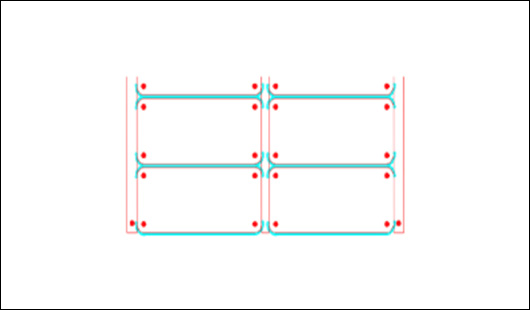
Both V-scoring and tab-routing techniques can be used on a single board, as shown in the following picture. The board space should be greater than 2.0mm between each unit. Usually, the space of the V-scoring area should be 3.0mm, and the tab routing area should be 1.6mm.
Other specifications in panel
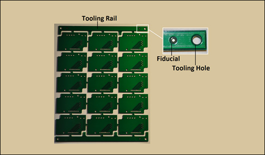
For each panel, there need at least three fiducial marks, and the diameter should be 1.0mm. Usually, the tooling holes should be set to 2.0mm, and the minimum tooling strip width is 5.0mm. Please contact us if you need more panel design tips.
Panel service in APOLLOPCB
PCB assembly panel with a minimum size of 75mm*75mm and a maximum size of 600mm* 500mm can be produced in APOLLOPCB. You can choose one of these board types when you run an online quote on our website: single piece, panel by customers, and panel by APOLLOPCB. If you have any idea about the panel design of your order, please contact our online service or send E-mails to info@apollopcb.com.

Got project ready to assembly? Contact us: info@apollopcb.com


We're not around but we still want to hear from you! Leave us a note:

Leave Message to APOLLOPCB
