-
- PCB TYPE
- PRINTED CIRCUIT BOARD PROTOTYPE ALUMINUM PRINTED CIRCUIT BOARD R&F PCB FPC HIGH FREQUENCY PCB HIGH-TG PCB HEAVY COPPER PCB HDI PCB PCB FOR LIGHTING METAL CORE PCB
Real PCB &PCB Assembly Manufacturer
IS09001:2015 Standard
UL.RoHS. REACH Certified
3000+ Orders/Day
99% on-time Shipping
100,000+ Customers
Panel creation means aggregating multiple PCBs on one large panel to manufacture. This large board is called a panel. You may notice that there always is a selection of board types when you place orders: a single board or panel design. Most of the time, people will choose panel design to save cost, unless the board is too big for the panel or there are special requirements.
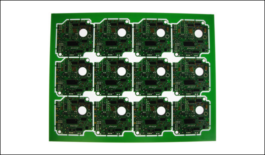
The reasons for panel creation
l Improve manufacturing efficiency and yield
l Provide convenience for SMT assembly and testing
l Material-saving and cost-saving
Panel types
Generally, PCB manufacturers provide you with panel service for free and also can produce the boards according to your panel design. There are several panel types for you to choose from, and all the panel techniques are easy for you to separate the boards into single boards.
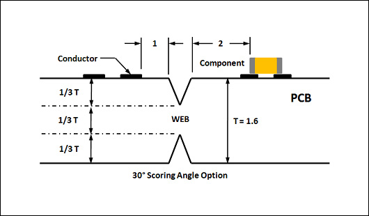
1. V-scoring/V-cut/V-groove
There is a V-shaped slot between the boards cut with a V-cut machine, which can be easily broken when used. V-scoring is suitable for the regular shaped PCBs with straight edges because the V-scoring machine will go through the whole board without stopping when running.
2. Routing slot/milling slot +Tab (Tab-routing)
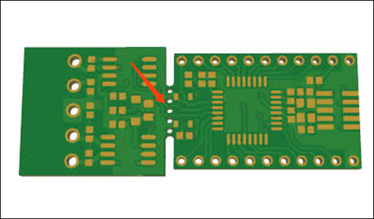
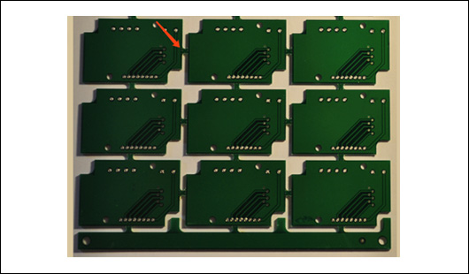
Routing slot is also called a milling slot, and it means there is a slot milled with a milling machine between the boards. And there is a tab in the middle of the slot. There are two kinds of tab-routing:
--Tab-routing with breaking holes
PCB units with different sizes are also more suitable for this technique. The edges of the two boards are connected by many small holes like stamp holes, which is easy to break.
Tab-routing without holes
3. The combination of V-scoring and tab-routing
For the consideration of PCB manufacturing, sometimes there need both V-scoring and tab-routing techniques on one panel.
Some panel rules and tips
l The panel shape should be as close to a square or rectangle as possible.
l The outer frame of the panel should be closed-loop, which can ensure that the PCB panel will not be out of shape after being fixed on the fixture.
l No large device or protruding component is allowed near the connection point between the outer frame and the inner board, and the connection point between each the inner board.
l Four fiducial holes are made at the corners of the outer frame, and the strength of the holes should be suitable to ensure that it will not break during the manufacturing process. The hole diameter and position accuracy should be high, and the walls of the hole should be smooth without burrs.
l When setting the fiducial points, usually leave a solderless area that is larger than 1.5mm around the fiducial mark.
Except for those mentioned above, there are many other rules and tips that should be considered when designing a panel for PCBs. If you have questions about the PCB panel design, contact us. Our maximum panel size is 500mm*600mm, the minimum size is 75mm*75mm, and the board separation way can be chosen from three methods: V-scoring, tab-routing, or none.

Got project ready to assembly? Contact us: info@apollopcb.com


We're not around but we still want to hear from you! Leave us a note:

Leave Message to APOLLOPCB
