-
- PCB TYPE
- PRINTED CIRCUIT BOARD PROTOTYPE ALUMINUM PRINTED CIRCUIT BOARD R&F PCB FPC HIGH FREQUENCY PCB HIGH-TG PCB HEAVY COPPER PCB HDI PCB PCB FOR LIGHTING METAL CORE PCB
Real PCB &PCB Assembly Manufacturer
IS09001:2015 Standard
UL.RoHS. REACH Certified
3000+ Orders/Day
99% on-time Shipping
100,000+ Customers
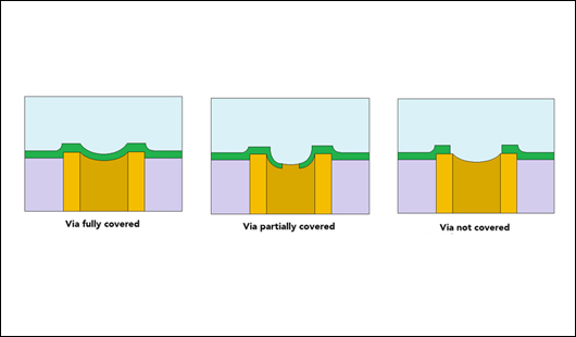
Via covering means that the vias are covered by the solder mask or other chemical materials. Why do the vias sometimes need to be covered in the PCB manufacturing process? Because the solder paste may get into the vias and cause short circuits if the through-holes are exposed. The condition in which the vias are not covered is called via opening.
Types of via covering
Usually, three types of the via covering are possible in PCB fabrication.
1. Via tenting
Via tenting means that the via is covered by a layer of solder mask. It is the simplest way of via covering. Generally, the vias using this covering type should not be greater than 0.3mm.
The solder mask can be applied on both sides of the PCB or only one-side of the PCB.

2. Via plugging
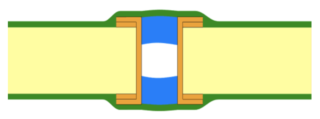
Via plugging is the case that the vias are partially closed with non-conductive media (epoxy/resin) and a layer of solder mask. There may also be no solder mask layer. Generally, the plugged vias should not be greater than 0.5mm. And multi-layer PCBs are recommended to do single-side via plugging.
The vias also can be filled double-sided or single-sided.

3. Via filling
Via filling indicate that the vias are fully filled with non-conductive materials. Sometimes there is another layer of solder mask over the non-conductive fillers.
There are two types of via filling:
l Via filling and covered via
The vias are filled with non-conductive media and covered with a layer of conventional solder mask.

l Via filling and capped via
Filling the via with non-conductive paste after the via is plated-through. Then metalizing and plating the via when the paste is hardened, and making the surface planar. The via surface is solderable in this situation and can increase additional traces between BGA vias.

The comparison of via covering types
Via filling is the most expensive and most reliable.
Via plugging is the most practical way, and it is cheaper than via filling.
Via tenting has the lowest price, but it may cause possible failures.
Keep the vias open on both sides is the easiest and cheapest method, but short circuits may exist in this situation. We recommend that you choose one the via covering type based on your budget and thequality requirement of the PCBs.


Got project ready to assembly? Contact us: info@apollopcb.com


We're not around but we still want to hear from you! Leave us a note:

Leave Message to APOLLOPCB
