-
- PCB TYPE
- PRINTED CIRCUIT BOARD PROTOTYPE ALUMINUM PRINTED CIRCUIT BOARD R&F PCB FPC HIGH FREQUENCY PCB HIGH-TG PCB HEAVY COPPER PCB HDI PCB PCB FOR LIGHTING METAL CORE PCB

Choose a reliable aluminum pcb manufacturer for LED and power. Learn high reflective soldermask options, material choices (GDM, Ventec), and how to quote fast.
Explore the advantages of aluminum pcb in LED and high-power applications. Learn about aluminum pcb stackup, aluminium-based CCL, and high thermal solutions.
Custom aluminum base PCB (MCPCB) for high-power designs—stable thermal performance, strict QC, prototype to volume. Get a fast quote for LED and power applications.
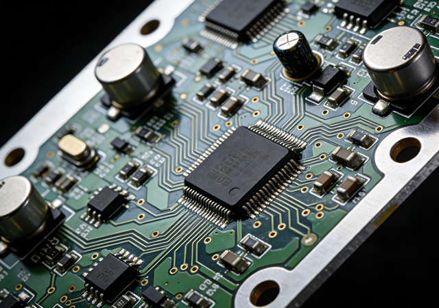
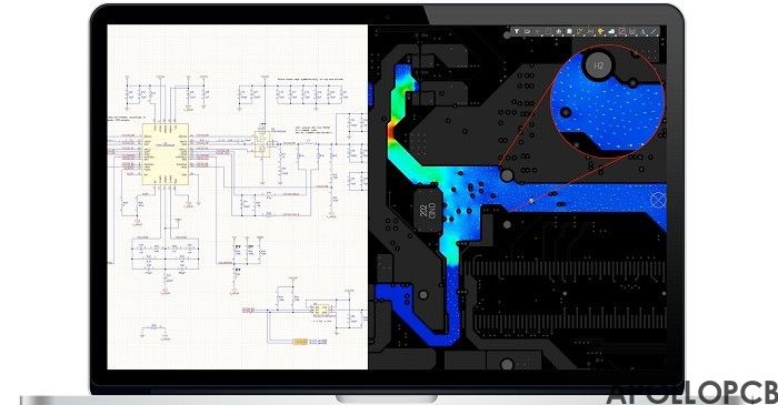
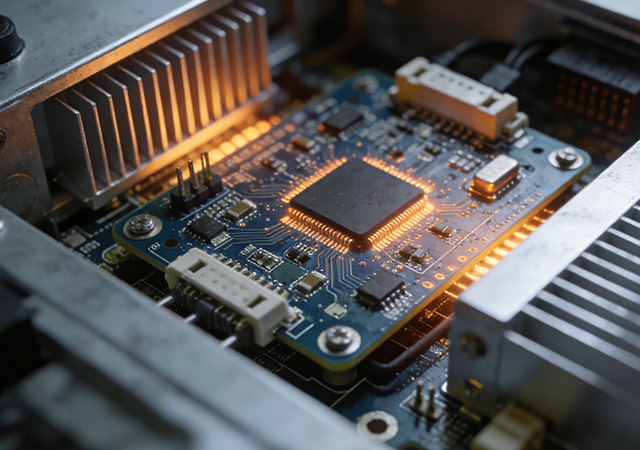
If you’re sourcing an aluminum pcb for high-power LED lighting or power electronics, the real success metric isn’t “cheap per panel”—it’s thermal performance, flatness during assembly, stable quality control, and lead-time reliability. Metal-core PCBs (MCPCB / IMS) are built to move heat away from hotspots far more effectively than standard FR-4, making them a common choice in LED lighting and power supplies where heat is a major factor.This article is written for factory buyers and engineers evaluating an aluminum pcb manufacturer (including aluminum pcb china sourcing), and it also covers advanced routing options such as blind and buried vias aluminum pcb for compact, high-density designs.
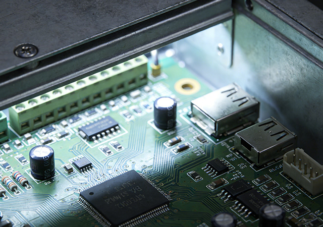
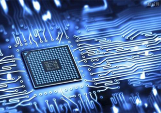
In today’s electronics industry, thermal management is a critical factor for ensuring the efficiency and longevity of high-power devices. Traditional PCBs, made of materials like FR-4, often struggle to handle the heat generated by power-sensitive components. This is where aluminum PCBs come in. With their superior thermal conductivity, mechanical strength, and cost-effectiveness, aluminum PCBs have become the go-to choice for a wide range of high-power electronic applications, particularly in LED lighting and power electronics.

Got project ready to assembly? Contact us: info@apollopcb.com


 Whatsapp 0086 755 29438407
 Mail info@apollopcb.com
 Tel 0086 755 29438407


ABOUT US

PRODUCTS
TECHNOLOGY
KNOWLEDGE CENTRE
CULTURE
NEWS
We're not around but we still want to hear from you! Leave us a note:

Leave Message to APOLLOPCB