-
- PCB TYPE
- PRINTED CIRCUIT BOARD PROTOTYPE ALUMINUM PRINTED CIRCUIT BOARD R&F PCB FPC HIGH FREQUENCY PCB HIGH-TG PCB HEAVY COPPER PCB HDI PCB PCB FOR LIGHTING METAL CORE PCB

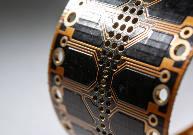
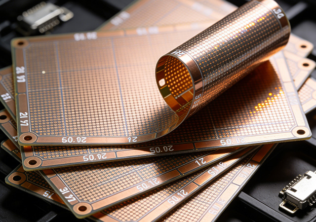
As the electronics industry evolves toward miniaturization, high-frequency operation, and multi-functional integration, the demand for flexible PCBs capable of supporting dense interconnections and reliable signal transmission has never been higher. Blind and Buried Vias Flexible PCB emerges as a pivotal solution, integrating blind vias (connecting surface and inner layers) and buried vias (linking inner layers exclusively) into flexible substrates to overcome the limitations of traditional through-hole designs. Unlike standard flexible PCBs, this advanced technology achieves superior space utilization, minimized signal loss, and enhanced mechanical flexibility—critical for powering 5G communication, autonomous driving, and wearable smart devices. For electronics manufacturers pursuing innovation in high-performance, compact products, Blind and Buried Vias Flexible PCB has become an indispensable core component.
Expert Medical Grade Vias Flexible PCB manufacturer. Specialized in high-reliability flex circuits for surgical tools, implants & diagnostics. Ensure ISO 13485 compliance with ApolloPCB—Get a quote!
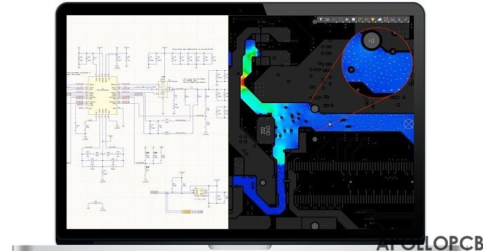
Leading HDI Blind & Buried Vias Flexible PCB manufacturer. Optimize signal integrity & space for next-gen smartphones, wearables & IoT. Explore ApolloPCB’s precision via technology—Get a 24h quote!
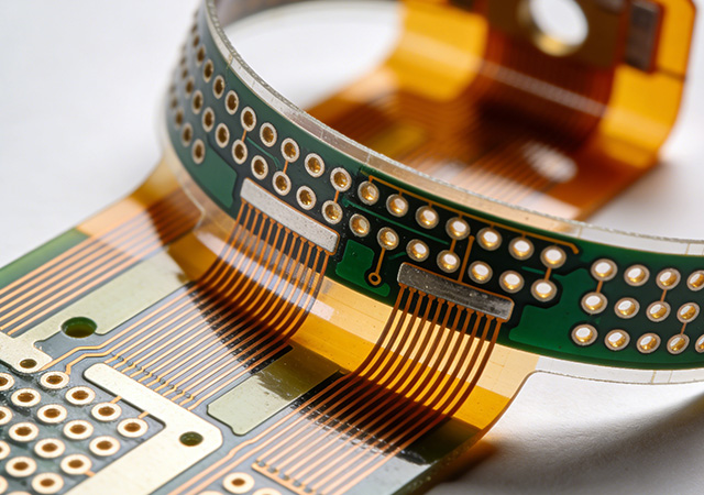
As electronic devices evolve toward miniaturization, flexibility, and multi-functionality, Flexible PCB (FPC) has become a core component supporting industrial upgrading in consumer electronics, automotive electronics, and medical devices. The traditional manufacturing model of FPC, however, has long been plagued by challenges such as low production efficiency, high defect rates, and difficulty in balancing mass production and customization. In recent years, advanced manufacturing technologies represented by laser welding and roll-to-roll production have brought revolutionary changes to the FPC industry. These innovations not only solve the core pain points of traditional manufacturing but also enable FPC to meet the diverse needs of emerging applications. For electronics manufacturers, understanding the advanced manufacturing trends of Flexible PCB is crucial to improving product competitiveness and seizing market opportunities.
As global industries pursue high reliability, safety, and sustainability, Polyimide (PI) has emerged as a cornerstone high-performance polymer material, redefining the performance boundaries of components in extreme environments. Renowned for its exceptional thermal stability, chemical resistance, and structural versatility, Polyimide transcends the limitations of traditional materials, enabling innovations in energy storage, aerospace, protective equipment, and advanced electronics. Unlike conventional polymers that compromise on performance under harsh conditions, Polyimide maintains consistent functionality across wide temperature ranges and corrosive environments, making it indispensable for mission-critical applications. For industries striving to address safety challenges and achieve carbon neutrality goals, leveraging Polyimide’s unique properties and innovative forms has become a strategic imperative.

Got project ready to assembly? Contact us: info@apollopcb.com


 Whatsapp 0086 755 29438407
 Mail info@apollopcb.com
 Tel 0086 755 29438407


ABOUT US

PRODUCTS
TECHNOLOGY
KNOWLEDGE CENTRE
CULTURE
NEWS
We're not around but we still want to hear from you! Leave us a note:

Leave Message to APOLLOPCB