-
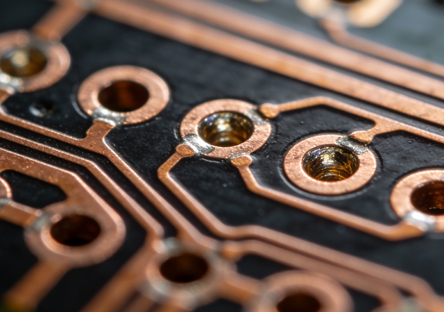
- PCB TYPE
- PRINTED CIRCUIT BOARD PROTOTYPE ALUMINUM PRINTED CIRCUIT BOARD R&F PCB FPC HIGH FREQUENCY PCB HIGH-TG PCB HEAVY COPPER PCB HDI PCB PCB FOR LIGHTING METAL CORE PCB

Enable extreme miniaturization with ApolloPCB’s Blind & Buried Vias FPCB. Optimize space & signal performance for wearables & high-density electronics. Reliable multi-layer flex circuits—Get a quote!
Boost RF performance with ApolloPCB’s Blind Vias FPCB. Minimize signal loss & stubs for 5G, IoT & radar systems. High-frequency precision engineering—Get your RF FPC quote now!
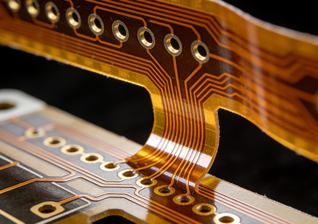
As electronic devices evolve toward higher integration, smaller form factors, and enhanced performance, the demand for advanced flexible printed circuit board (FPCB) design solutions has never been greater. Among these innovations, HDI Blind/Buried Vias FPCB Design stands out as a transformative approach, redefining the boundaries of precision and miniaturization in flexible electronics. Unlike traditional FPCB designs, HDI Blind/Buried Vias FPCB Design leverages high-density interconnect (HDI) technology with blind and buried vias to optimize circuit layout, reduce signal loss, and maximize space utilization. This specialized design solution has become indispensable for high-end electronic products that require both flexibility and ultra-high performance, making it a key focus for engineers and manufacturers across industries.
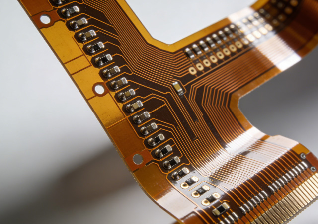
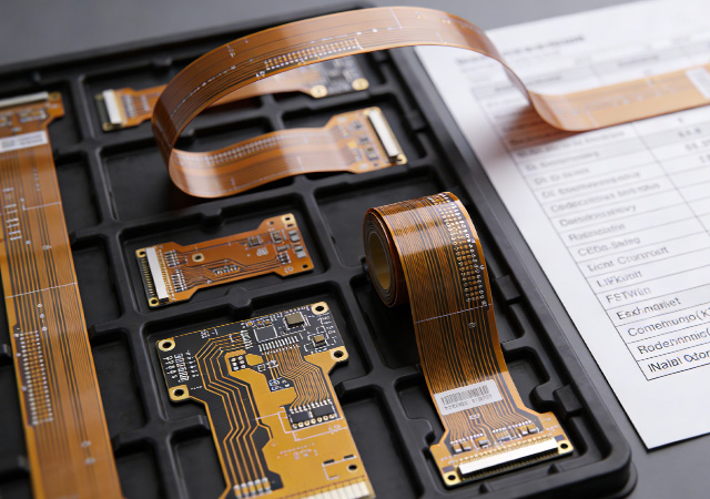
In the era of smart and portable electronics, the demand for components that combine compactness, versatility, and durability has redefined the boundaries of electronic design. Flexible Printed Circuit Board (FPCB) has emerged as a transformative technology, breaking the limitations of traditional rigid PCBs and becoming the core enabler of next-generation electronic products. FPCB’s unique ability to bend, fold, and conform to irregular shapes while maintaining stable electrical performance has made it indispensable across industries, from consumer tech to healthcare and automotive. As innovation accelerates, FPCB continues to reshape how electronic devices are designed, manufactured, and used, solidifying its position as a cornerstone of modern electronics.
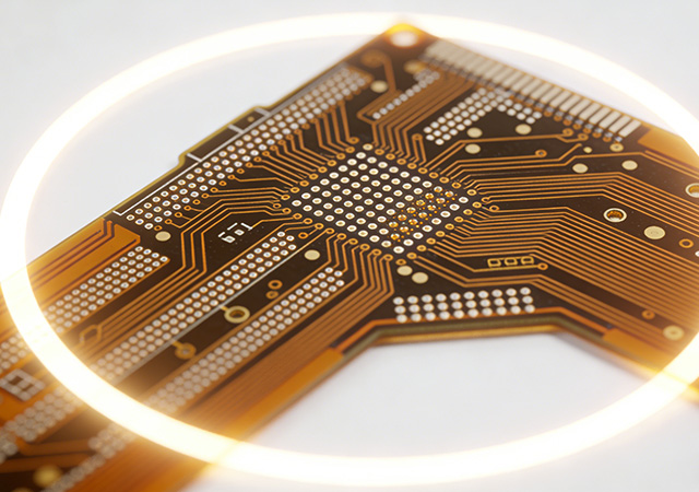
In the fast-evolving electronics industry, flexible printed circuit boards (FPCBs) have become indispensable components, enabling the design of compact, versatile, and high-performance devices. Behind every successful FPCB-powered product lies a reliable fpcb supplier— a partner that bridges design concepts with practical manufacturing, ensuring consistent quality, technical support, and timely delivery. As industries ranging from consumer tech to healthcare and automotive pursue innovation, the role of an fpcb supplier has evolved from a mere component provider to a strategic collaborator. Choosing the right fpcb supplier is no longer a transactional decision but a critical step in enhancing product competitiveness and accelerating time-to-market.

Got project ready to assembly? Contact us: info@apollopcb.com


 Whatsapp 0086 755 29438407
 Mail info@apollopcb.com
 Tel 0086 755 29438407


ABOUT US

PRODUCTS
TECHNOLOGY
KNOWLEDGE CENTRE
CULTURE
NEWS
We're not around but we still want to hear from you! Leave us a note:

Leave Message to APOLLOPCB