-
- PCB TYPE
- PRINTED CIRCUIT BOARD PROTOTYPE ALUMINUM PRINTED CIRCUIT BOARD R&F PCB FPC HIGH FREQUENCY PCB HIGH-TG PCB HEAVY COPPER PCB HDI PCB PCB FOR LIGHTING METAL CORE PCB

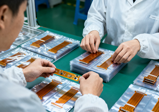
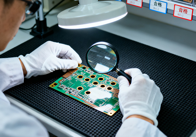
In the fast-paced global electronics market, where product lifecycles are shortening and customer demands are increasingly diverse, a professional FPC manufacturer stands out as a strategic partner rather than a mere component supplier. Specializing in flexible printed circuits (FPCs)—the foundational components enabling flexible, compact, and multi-functional electronic designs—top FPC manufacturers differentiate themselves through agile supply chain management and deep customization capabilities. Unlike generic component manufacturers, they can quickly adapt to market changes, tailor FPC solutions to specific application needs, and ensure compliance with global industry regulations. For enterprises ranging from startups to Fortune 500 companies, partnering with such an FPC manufacturer is critical to accelerating product development, reducing market risks, and maintaining competitive advantage.
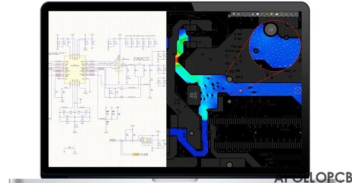
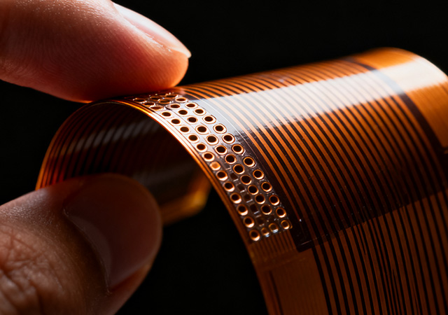
As electronic devices evolve toward ultra-miniaturization, high integration, and high-frequency operation, the demand for flexible printed circuits (FPCs) with blind and buried vias has surged dramatically. A professional Blind and Buried Vias FPC Manufacturer specializes in the design and production of FPCs integrated with blind vias (connecting surface to inner layers) and buried vias (connecting only inner layers), which are pivotal for optimizing circuit density, reducing signal loss, and enhancing design flexibility. Unlike standard FPC manufacturers focusing on through-hole vias, these specialized manufacturers possess unique expertise in blind and buried via fabrication, high-density routing, and signal integrity optimization—critical for powering next-generation devices in 5G communications, automotive electronics, and precision medical equipment. Partnering with a reputable Blind and Buried Vias FPC Manufacturer is essential for enterprises aiming to translate innovative high-
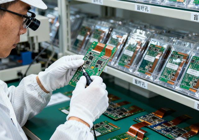
In electronic systems where failure is intolerable—such as aerospace, medical devices, and industrial control—the role of a High Reliability Vias FPC Maker becomes irreplaceable. A professional High Reliability Vias FPC Maker specializes in designing and manufacturing flexible printed circuits (FPCs) with high-integrity vias (including blind, buried, and through vias) that ensure long-term stability and performance under extreme conditions. Unlike standard FPC manufacturers, these specialized makers prioritize via reliability through advanced fabrication processes, rigorous quality validation, and material optimization, ensuring their FPCs can withstand harsh environments such as extreme temperatures, vibration, humidity, and chemical exposure. For enterprises developing mission-critical electronic products, partnering with a reputable High Reliability Vias FPC Maker is a foundational step to safeguarding product safety, performance, and brand reputation.
The rapid advancement of radio frequency (RF) technologies—from 5G/6G communications to automotive radar and industrial IoT—has placed unprecedented demands on flexible printed circuits (FPCs). Blind Buried Vias FPC for RF emerges as a specialized solution tailored to the unique requirements of RF applications, where signal integrity, electromagnetic compatibility (EMC), and space efficiency are critical. Unlike standard FPCs with through-hole vias, this advanced FPC integrates blind vias (connecting surface layers to inner layers) and buried vias (connecting only inner layers) to optimize RF signal paths, minimize signal loss, and reduce electromagnetic interference (EMI). For manufacturers of RF devices, partnering with providers of high-quality Blind Buried Vias FPC for RF is essential to unlocking the full potential of next-generation high-frequency electronic systems.
As the global electronics industry embraces the dual trends of digital transformation and green sustainability, the role of a professional FPC manufacturer has evolved beyond component production to become a catalyst for eco-friendly and technologically advanced flexible electronics. An FPC manufacturer specializing in sustainable innovation integrates environmentally responsible practices with cutting-edge manufacturing technologies, delivering flexible printed circuits (FPCs) that balance performance, reliability, and environmental impact. Unlike traditional FPC suppliers, these forward-thinking manufacturers prioritize green material adoption, energy-efficient processes, and circular economy principles, while adapting to the evolving needs of emerging technologies such as AIoT, 6G, and smart mobility. For enterprises pursuing carbon neutrality goals and technological leadership, partnering with a reputable FPC manufacturer with strong sustainability and innovation capabilities is a

Got project ready to assembly? Contact us: info@apollopcb.com


 Whatsapp 0086 755 29438407
 Mail info@apollopcb.com
 Tel 0086 755 29438407


ABOUT US

PRODUCTS
TECHNOLOGY
KNOWLEDGE CENTRE
CULTURE
NEWS
We're not around but we still want to hear from you! Leave us a note:

Leave Message to APOLLOPCB