-
- PCB TYPE
- PRINTED CIRCUIT BOARD PROTOTYPE ALUMINUM PRINTED CIRCUIT BOARD R&F PCB FPC HIGH FREQUENCY PCB HIGH-TG PCB HEAVY COPPER PCB HDI PCB PCB FOR LIGHTING METAL CORE PCB

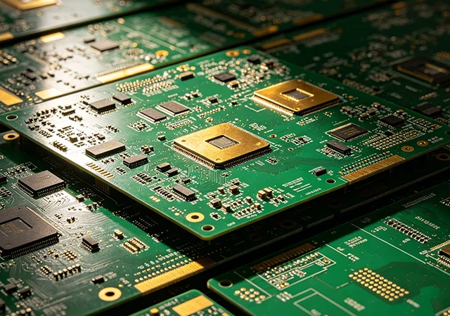
Explore why FR4 PCB is the industry standard. Learn about signal integrity, High-Tg materials, and precision fabrication for modern high-performance electronics.
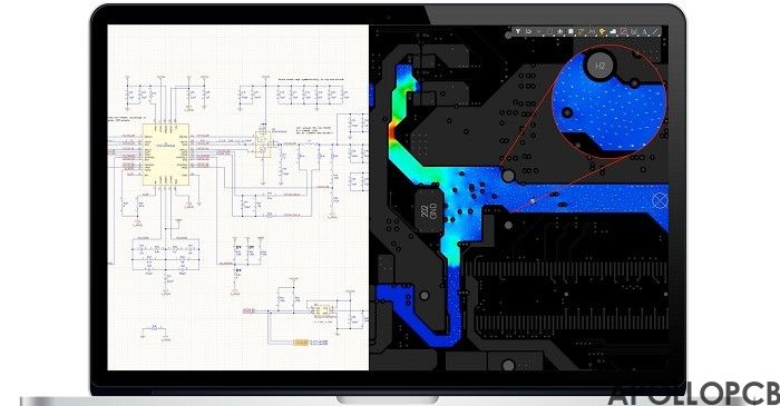
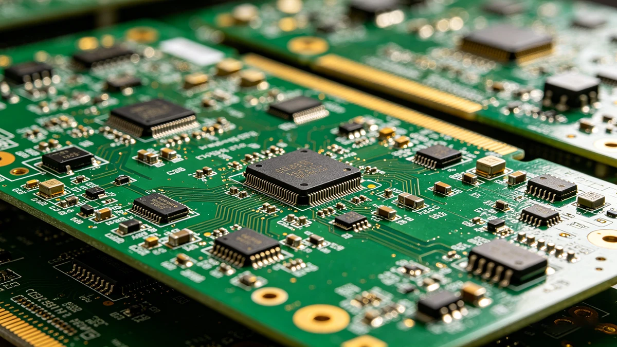
Discover how ApolloPCB achieves micron-level precision in multi-layer FR4 PCB manufacturing. From LDI alignment to High-Tg solutions, we ensure high reliability for your complex designs. Read our expert manufacturing guide.
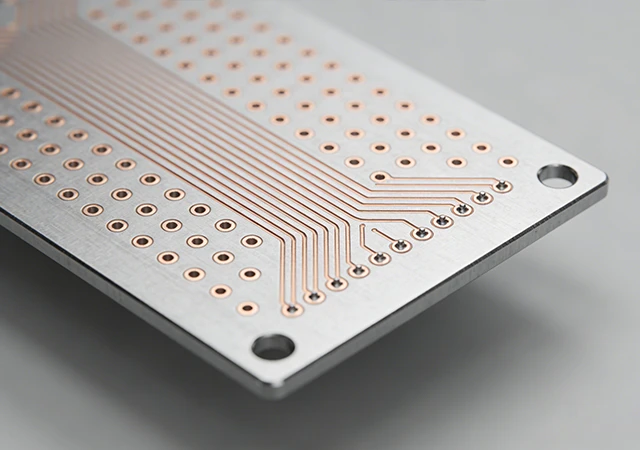
Get custom aluminum PCB solutions with IATF 16949 quality. ApolloPCB offers 24-72h turnaround for high-performance MCPCBs and automotive electronics.
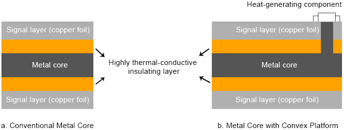
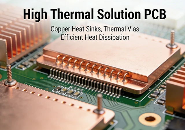
Discover how Aluminum PCBs revolutionize heat dissipation in high-power LEDs and Automotive systems. Learn about thermal conductivity, material selection (Ventec, GDM), and why ApolloPCB is the leader in high-performance MCPCB solutions.
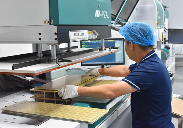
Explore the expert world of Aluminum PCB manufacturing. From 8.0 W/m·K thermal conductivity to specialized countersink holes, learn how ApolloPCB ensures zero-defect production for LED and automotive systems. China's top MCPCB factory.

Got project ready to assembly? Contact us: info@apollopcb.com


 Whatsapp 0086 755 29438407
 Mail info@apollopcb.com
 Tel 0086 755 29438407


ABOUT US

PRODUCTS
TECHNOLOGY
KNOWLEDGE CENTRE
CULTURE
NEWS
We're not around but we still want to hear from you! Leave us a note:

Leave Message to APOLLOPCB