-
- PCB TYPE
- PRINTED CIRCUIT BOARD PROTOTYPE ALUMINUM PRINTED CIRCUIT BOARD R&F PCB FPC HIGH FREQUENCY PCB HIGH-TG PCB HEAVY COPPER PCB HDI PCB PCB FOR LIGHTING METAL CORE PCB

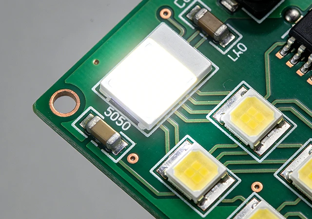
Comprehensive SMD LED package size specifications (0603, 0805, 1206, etc.). Optimize your LED PCB design with our assembly guide. Perfect for lighting and industrial displays.
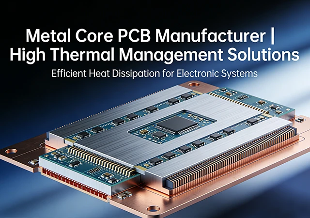
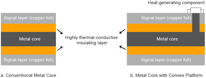
Eliminate heat issues with a leading Metal Core PCB manufacturer. ApolloPCB provides high-thermal management solutions (up to 4.0 W/m·K) for LED, automotive, and power tech. Get expert DFM support and fast-turn MCPCB fabrication today.
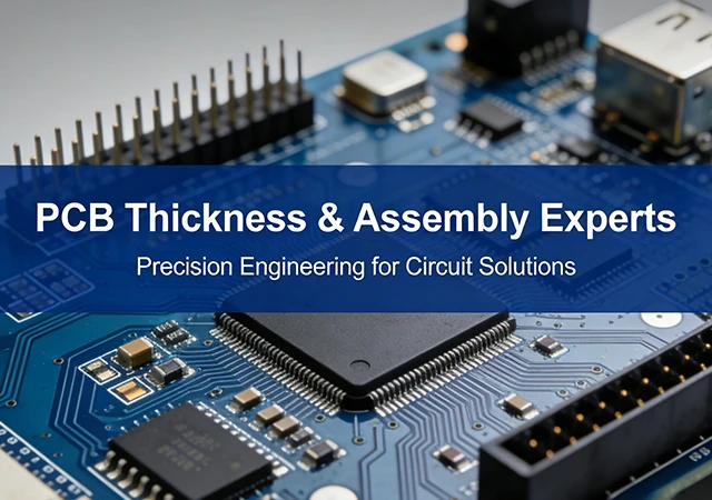
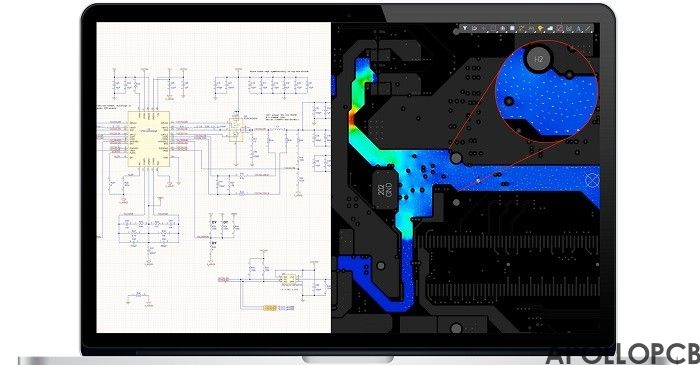
Struggling with space constraints? ApolloPCB specializes in custom PCB thickness from 0.2mm to 6.0mm. Full turnkey assembly for FR4, Aluminum, and Flex PCBs with IPC Class 3 precision. Optimize your high-density designs with our 10-year expert team today.
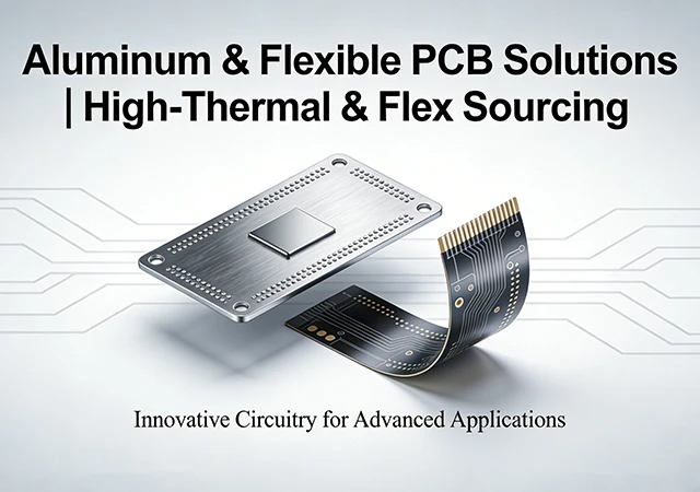
Solve heat and space constraints with ApolloPCB. We offer high-thermal conductivity Aluminum PCBs and ultra-reliable Flexible PCB (FPC) solutions. From prototyping to assembly for LED, automotive, and IoT tech. Secure your specialized PCB sourcing today.
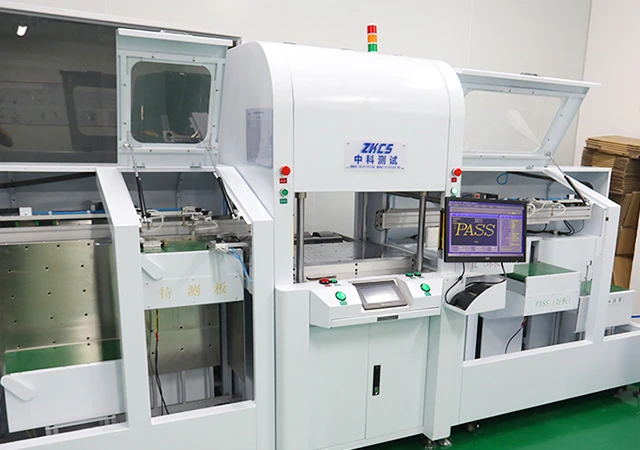
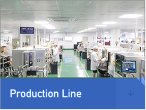
Explore ApolloPCB’s state-of-the-art manufacturing facility. From high-speed SMT lines to precision CNC drilling and X-ray inspection, discover the equipment that guarantees IPC Class 3 quality for your industrial PCB projects. Get a free quote today.

Got project ready to assembly? Contact us: info@apollopcb.com


 Whatsapp 0086 755 29438407
 Mail info@apollopcb.com
 Tel 0086 755 29438407


ABOUT US

PRODUCTS
TECHNOLOGY
KNOWLEDGE CENTRE
CULTURE
NEWS
We're not around but we still want to hear from you! Leave us a note:

Leave Message to APOLLOPCB